Inside Apple’s A13 Bionic system-on-chip
Since the very first Apple-designed smartphone chip (the A4 back in 2010), the company has been a force to be reckoned with in mobile silicon design. It was with the A6 a couple years later, when Apple used its own CPU design instead of a licensed architecture, that its performance leadership really started to kick into high gear.
For the last several years, Apple’s CPU has really been untouchable. The A11 Bionic featured not only a custom Apple-designed CPU, but finally ditched the PowerVR-based graphics processor for its own custom GPU. In addition, it introduced the Neural Engine, a custom block of silicon separate from the CPU and GPU, focused on accelerating Machine Learning computations.
Since that time, Apple’s mobile silicon has held court over the smartphone chip world. Maybe the iPhone doesn’t have the fastest cellular speeds in the business, but Apple is determined to make sure that nobody is going to have a faster CPU, GPU, or machine learning acceleration.
The year-old A12 Bionic is still faster in many ways than the chip in any Android phone, and the A13, debuting in the
iPhone 11 and
iPhone 11 Pro, is considerably faster. Here are all the improvements that make the A13 Bionic—once again—the chip to beat in the smartphone race.
Mục Lục
Bleeding-edge 7nm+ process
Apple always uses the very best manufacturing process technology available from its foundry partners (which has almost always been TSMC). Today, that means it is among the first to use TSMC’s new second-generation 7 nanometer process. It’s similar to the 7nm process that availed itself so well in last year’s A12 Bionic and processors like AMD’s
Ryzen 3000 series.
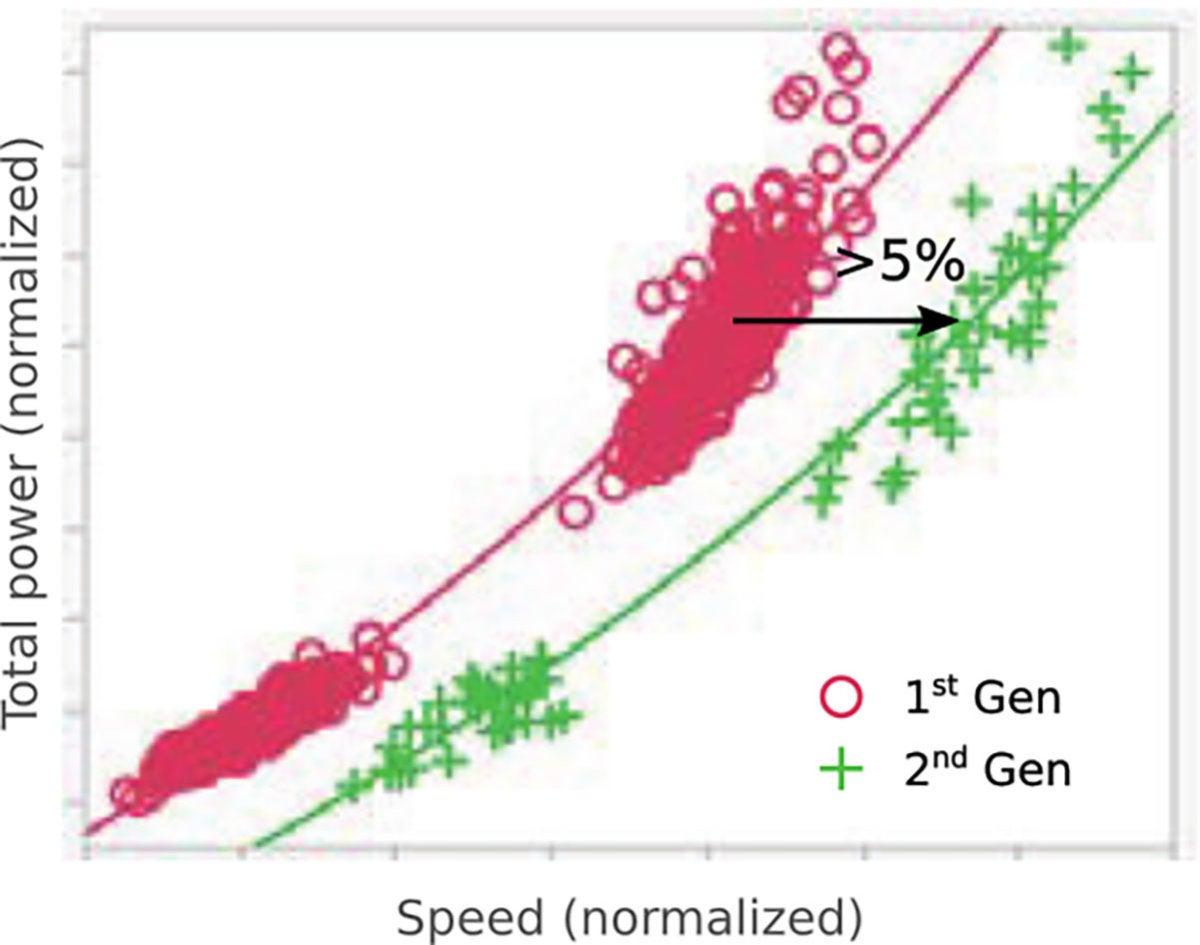
The second-generation process, sometimes referred to as 7nm+ or 7NP, etches some of the chip layers with extreme ultraviolet lithography (EUV). That means smaller, more tightly packed transistors that leak less power.
 TSMC
TSMC
The second-generation 7nm process from TSMC uses partial EUV technology to make faster, more power-efficient transistors.
In practice, it means a bit more transistors in the same space, but also higher clock speeds at the same power draw, or less power draw at the same clock speeds. That’s exactly what we see in the A13 Bionic.
Apple crammed 8.5 billion transistors in the A13, an increase of 23 percent over the A12. The chip is estimated to be around 20 percent larger—about 98 mm², compared to 83 mm² for the A12. Thus, Apple achieved only a small increase in density, but a big increase in maximum performance and power efficiency.
This is not Apple’s biggest chip ever, however. The A12X found in the new iPad Pro has more transistors (10 billion) and is estimated to be around 135 mm², and both the A5 and A10 Fusion were over 120 mm².
The fastest CPU gets faster
Apple’s custom CPU designs regularly deliver faster single-core performance than any competing smartphone chip, though benchmarks are hard to rely on when you’re talking about totally different platforms. Multi-core performance is hard to beat, too.
The tradition continues with the A13 Bionic. Apple says that both its two large high-performance CPU cores and the four energy-efficient CPU cores are 20 percent faster than those in the A12.
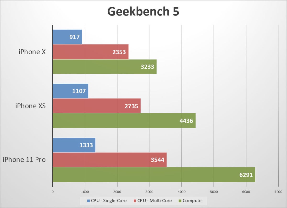
CPU performance is the best in the business. No Android phone gets close to these numbers.
In the real world, you almost never actually see the maximum theoretical performance increase, but our benchmarks showed CPU performance increases of right around 20 percent, with multi-core performance climbing even higher.
This is a superb year-on-year performance increase, and it’s going to be quite a challenge for Qualcomm, Samsung, and the like to match it.
Catching up and pulling ahead in GPU performance
If there’s one area where competing smartphone processors have been able to beat Apple, it’s in graphics performance. Apple’s GPUs deliver real-world performance that is among the best in the business, but some cross-platform benchmarks will favor the latest Android phones.
The GPU in the A13 is still the a custom quad-core Apple design, which Apple claims is “metal optimized” and 20 percent faster. In our tests, it was much faster than that. The compute performance in Geekbench, which uses the Metal API on the GPU, ran about 40 percent faster in both Geekbench 4 and Geekbench 5.
 IDG
IDG
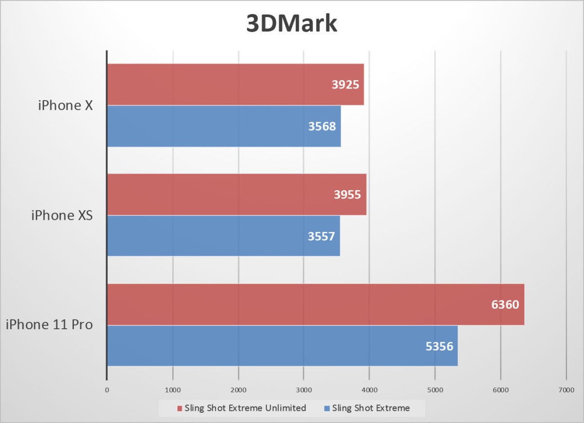
The high-end 3D Mark Five Strike test didn’t improve much last year, but took a big leap forward with the A13.
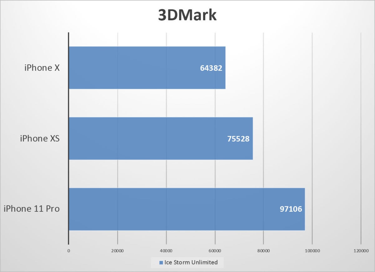
The 3DMark Fire Strike tests we ran were 50 to 60 percent faster (a good measure of modern high-end 3D game performance). Older 3DMark Ice Storm Unlimited ran almost 30 percent faster; Apple’s chips already blew alway the competition in this test, and at this point are just running up the score.
 IDG
IDG
The older Ice Storm Unlimited test didn’t improve by as much as the Fire Strike test, but it’s already much faster than other smartphone chips.
If you look at the combination of GPU compute performance and gaming-class 3D benchmarks, it’s fair to say that Apple’s go the fastest overall GPU in a smartphone right now. It is a closer call than CPU performance, though, and easier to see a competitor stealing the crown before the introduction of the A14 in the fall of 2020.
It’s really interesting that we’re seeing real-world performance far in excess of Apple’s 20 percent improvement claim. It’s hard to know what’s responsible for this, but I theorize that it has to do more with memory bandwidth than peak GPU theoretical performance.
Apple claimed that the A12 delivered up to 50 percent faster GPU performance than the A11, but we saw nothing of the sort—some tests didn’t show any real improvement at all. We guessed, at the time, that limitations of memory bandwidth were keeping the chip from achieving its top theoretical performance in some 3D graphics tests. Perhaps this year, though the chip isn’t 50 percent “faster,” it is better able to use the available memory bandwidth.
Whatever the reason, Apple is realizing way more than the promised 20 percent improvement in GPU performance.
Better power efficiency
Perhaps just as impressive as the performance improvements in the A13 Bionic is the increase in energy efficiency. Apple says the A13’s GPU and high-efficiency CPU cores use 40 percent lower power, while the high-performance CPU cores use 30 percent less and the Neural Engine uses 15 percent less.
Those figures come with a big huge asterisk, however. That is the power saving when delivering the same performance as the A12 Bionic. In other words, when the A13’s parts run at the same speed as the A12’s, they use that much less power. When they run faster, those power savings are greatly diminished.
 IDG
IDG
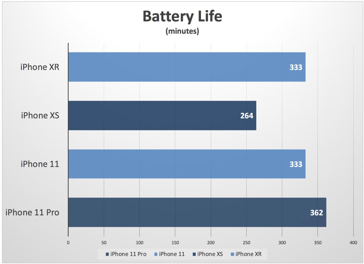
In benchmarks, the iPhone 11’s battery life is about equal to the iPhone XR (despite being much faster). In real daily use, we found it to last longer.
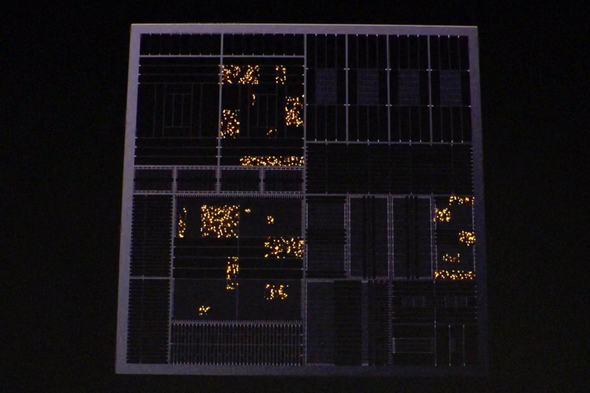
Apple says this is achieved partly by having hundreds of voltage domains to lower power to major parts of the chip when not in use, and hundreds of thousands of clock-gating domains, to disable logic gates that aren’t in use. That sounds impressive, but honestly, it’s a pretty standard part of modern top-tier chip design. Perhaps Apple goes further with these design elements than competing products—without precise figures it’s impossible to know–but this shouldn’t be viewed as a special new innovation.
Apple
Voltage and clock domains ensure that parts of the chip that aren’t in use in this precise microsecond don’t waste any power.
All those caveats aside, the performance-per-watt of the A13 is an impressive leap over the A12. Despite having similar-sized batteries, an identical display, and delivering a lot more performance, the iPhone 11 lasted just as long as the iPhone XR in our Geekbench 4 constant-benchmark battery test. In daily use, the battery lasts longer, which is perhaps the best indicator of all. The iPhone 11 Pro lasts a lot longer than the iPhone XS, but that is not solely due to the more efficient A13 chip—the display is also more efficient, and the battery is a lot larger.
It’s difficult to eliminate all the variables necessary to give a true apples-to-apples power efficiency comparison between chips that are locked into different phones. But the worst thing one might say about A13 Bionic’s power efficiency is that it appears to deliver significantly better performance while using a similar amount of power as the A12.
Made for Machine Learning
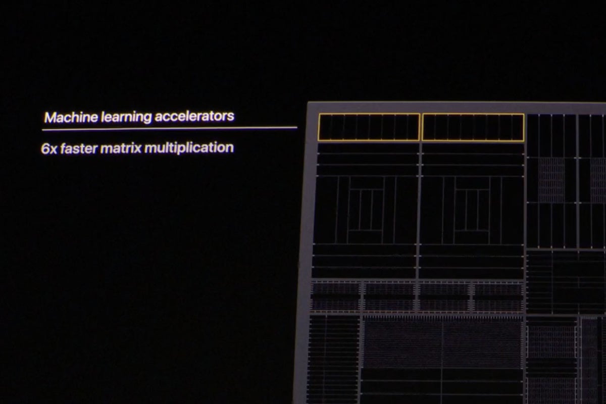
This year, the CPU has a new trick: A set of “machine learning accelerators” that perform matrix multiplication operations up to six times faster than the CPU alone. It’s not clear how exactly this hardware is accessed (are they extensions to the ARMv8 instruction set, like Intel’s AVX is to x86?), but for tasks like machine learning (ML) that use lots of matrix operations, the CPU is a powerhouse. Note that this matrix multiplication hardware is part of the CPU cores and separate from the Neural Engine hardware.
Apple
On one very particular type of math operation, the CPU is now up to six times faster.
The Neural Engine, like everything else in the chip, tops out at 20 percent faster than before (it’s as if the designs are relatively unchanged, and the new 7nm+ process allows for 20 percent higher clock speeds).
And the GPU, which Apple says is “metal optimized,” may or may not be a new design but it delivers faster compute performance using the Metal API in our testing.
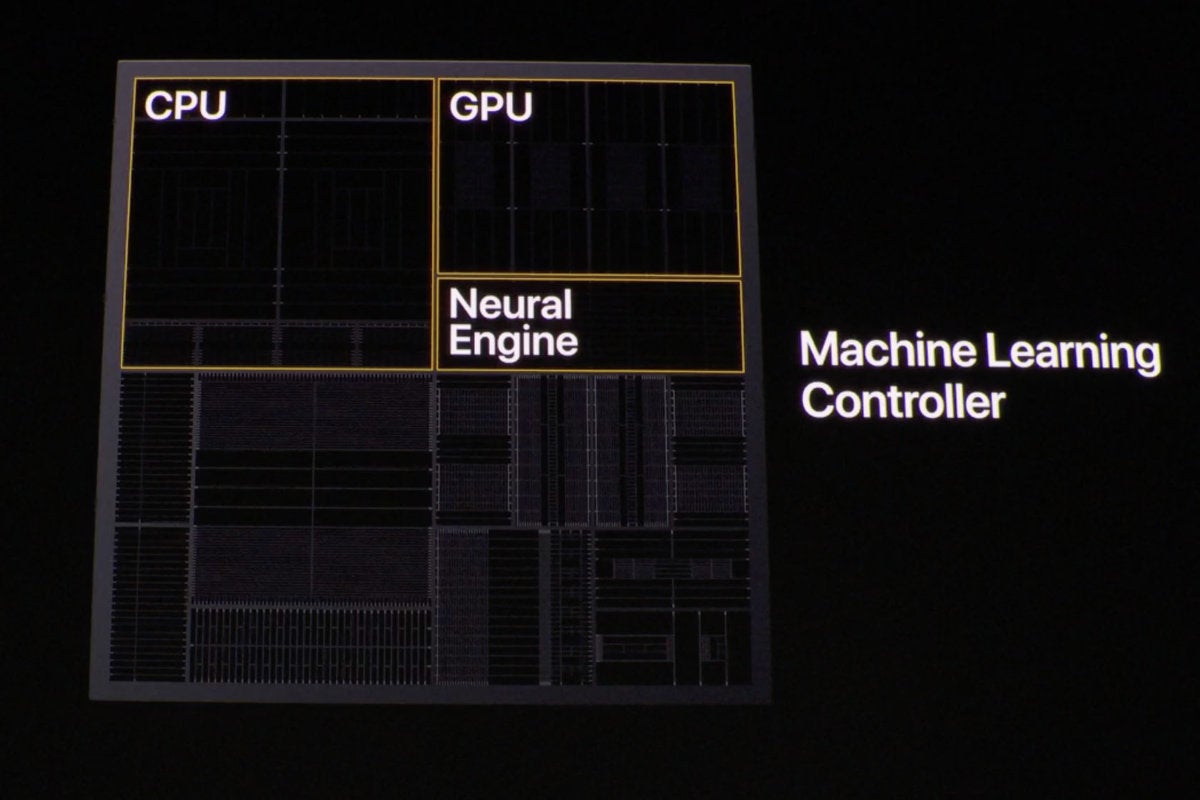
There’s a machine learning controller in the chip that automatically schedules machine learning operations between the CPU, GPU, and Neural Engine so developers don’t have to balance out the load themselves.
Apple
The CPU, GPU, and Neural Engine work together on machine learning tasks.
As a result of all this, machine learning code should run much faster on the A13 than on the A12.
The bar has been set
Months before the announcement of the new iPhones and their A13 Bionic chip, we
made a series of predictions about what we might expect.
We got the manufacturing process right, and were pretty close on the size (we estimated just over 100 mm²), but we overestimated the increased density of the 7nm+ process and thought Apple would field a 10 billion transistor processor, not 8.5 billion. We also assumed slightly better single- and multi-core performance, but underestimated just how much better the GPU would get. We also thought the Neural Engine would greatly expand. Instead, it is simply 20 percent faster like the rest of the chip, and Apple built dedicated matrix multiplication hardware into the CPU instead.
It’s still a little too early for us to form a set of predictions for the A14, except to say that we expect it to use TSMC’s most bleeding-edge process and be even faster and more power efficient. But as for the A13 Bionic, it once again sets the bar for smartphone SoCs. There may be one particular metric by which competing chips are faster, but nobody comes close to the intersection of CPU, GPU, and machine learning performance, not to mention all the dedicated functions for which Apple is among the best in the business (like image signal processing and video encoding).


