The ASUS Z170-A Motherboard Review: The $165 Focal Point
In the world of technology, you could speculate if there is ever a golden age, or a renaissance. All the time we expect technology to grow and improve, being better than the last. Sometimes there is nostalgia, but it never stops us using the latest because it provides the user experience we expect at a minimum. Like all the motherboard manufacturers, I’ve followed ASUS for years, and observed their constant iteration as platforms evolve. The newest Skylake platform is upon us, and we review the ASUS Z170-A motherboard to see their interpretation of the desktop this generation.
Mục Lục
Other AnandTech Reviews for Intel’s 6th Generation CPUs
100-Series Motherboard Reviews:
To read specifically about the Z170 chip/platform and the specifications therein, our deep dive into what it is can be found at this link.
ASUS Z170-A Overview
The motherboard industry has gone through years of consolidation and enhancement, making it very difficult for new companies to emerge. There is strong competition, profit margins are low, and there is a bare minimum expectation of utility. This is seen by the continual march on gaming branded motherboards, if only for SEO, or marketing label enhancements. Aside from ASUS’ Republic of Gamers brand, the channel line from ASUS remains free of the gaming SEO and promotes itself as a platform bundled with their self-proclaimed value additions, which can be condensed into ‘design, user requested software tools and user experience’. ASUS is not alone in this push, which makes the Z170-A an important part of ASUS’ product offering. At $165, it aims at a price point that end-users and system integrators alike will use for the majority of their i5 and i7 systems.
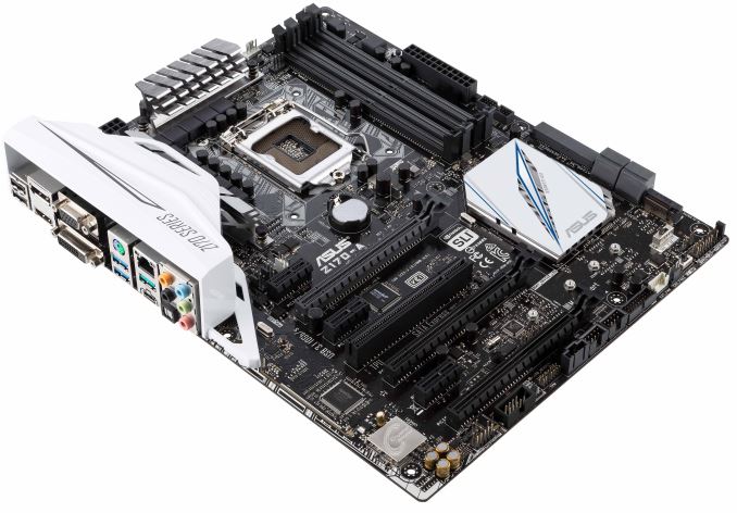
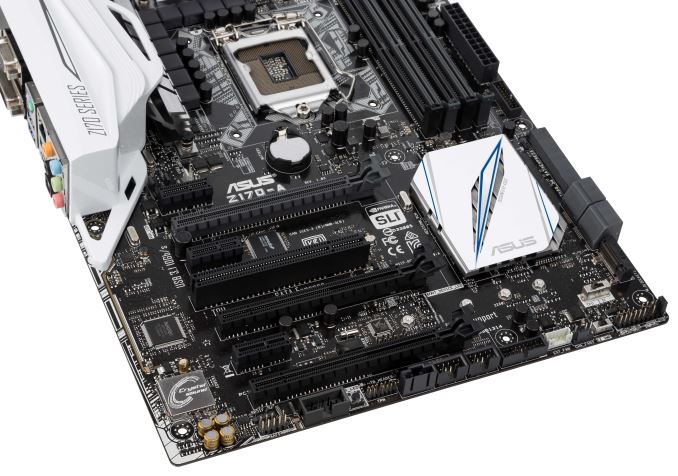
On the face of it, looking at the base hardware add-ons, the Z170-A comes in with a fair amount of what you expect at this price. Networking is the Intel I219-V controller, there is a single PCIe 3.0 x4 based M.2 slot, two USB 3.1 ports at 10 Gbps is provided by an ASMedia ASM1142 controller in both Type-A and Type-C formats, and the PCIe layout promotes two-way graphics with a tertiary PCIe 3.0 x4 slot from the chipset so SLI is not disrupted. One thing to note is the use of a Realtek ALC892 codec, which is perhaps a little surprising as there will be other motherboards around this price point that have the ALC1150.
ASUS’ marketed unique points include their onboard ICs to aid overclocking (TPU) and power (EPU), along with an onboard switch to help enable XMP on a memory kit without going into the BIOS. Building on this is a Pro-Clock IC that extends the overclocking range in the base frequency and a T-Topology memory trace design typically reserved for maintaining the high end desktop platform signal integrity (but is optional on Z170). The BIOS and software from ASUS has historically been positive, and we see this as a continuing trend with Skylake.
We worked with the Z170-A for part of our Skylake CPU coverage, as added information and BIOSes from ASUS on elements such as the FCLK issue and PCIe performance. The Z170-A, for the BIOSes tested, did not have multi core turbo but did give a 4.8 GHz overclock both in automatic and manual modes.
The $160-$170 price band will be hotly contested for both self-build and retailer pre-built designs. Here ASUS executes well with plenty of positives. For regular and power users, unless you want two M.2 devices or dual network ports, this board seems ideal for a shortlist.


Gallery: ASUS Z170-A
Quick Links to Other Pages
Page 2: Board Features and Visual Inspection
Page 3: BIOS
Page 4: Software
Page 5: System Performance (Audio, USB, Power, POST Times on Windows 7, Latency)
Page 6: CPU Performance, Short Form (Office Tests and Transcoding)
Page 7: Gaming Performance 2015 (R7 240, GTX 770, GTX 980)
Page 8: Conclusions
Quick Board Feature Comparison
Motherboard Comparison
ASUS Z170-A
Socket
LGA1151
LGA1151
MSRP at Review
$165
$230
DRAM
4 x DDR4
4 x DDR4
PCIe Layout
x8/x8
x8/x8
BIOS Version Tested
0603
142
MCT Enabled Automatically?
No
Yes
USB 3.1 (10 Gbps)
ASMedia ASM1142
1 x Type-A
1 x Type-C
ASMedia ASM1142
1 x Type-A
1 x Type-C
M.2 Slots
1 x PCIe 3.0 x4
2 x PCIe 3.0 x4
U.2 Ports
No
No
Network Controller
1 x Intel I219-V
1 x Killer E2400
Audio Controller
Realtek ALC892
Realtek ALC1150
HDMI 2.0
No
No
ASUS Z170-A Overclocking
Experience with ASUS Z170-A
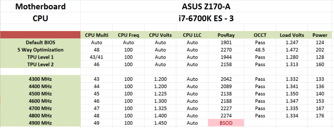
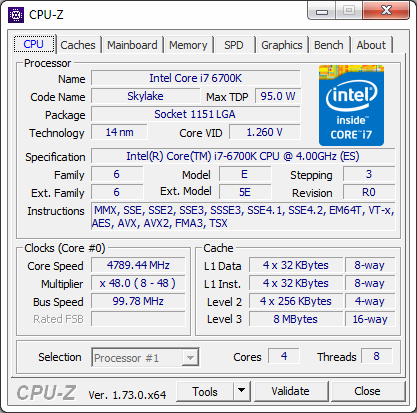
The Z170-A was the second motherboard we tested as part of the initial Skylake routine, partly due to the discussions we had behind some of the discrete PCIe co-processor performance on the Z170 platform. For overclocking, while the previous motherboard we had tested seemed happy moving around at 4.6 GHz for an overclock, the ASUS Z170-A went straight in at 4.8 GHz, no questions asked. It was quite a difference.
Through the Automatic overclock tool, we let it run and set a temperature limit of 90C for the intermediate stress testing, with each stress test lasting two minutes. I came back to the system about 15 minutes later to see the final results screen show the 4.8 GHz value. We validated this speed and it passed all of our tests, except video encoding. (We discussed the principles of stability in our Skylake overclock testing piece and suffice to say, there are two major camps on the issue.) The TPU Switch gave a good set overclocks as well, with the first stage giving 4.3 GHz/4.1 GHz split for +100 MHz (mild), and the second stage going up to 4.6 GHz on a single core turbo.
For manual overclocking, the results were almost the same, although we were able to get the same frequencies at a lower voltage and power which might be expected. We went for 4.9 GHz as well, but this failed regardless of voltage causing POV-Ray to crash and the system to bluescreen.
Methodology
Our standard overclocking methodology is as follows. We select the automatic overclock options and test for stability with POV-Ray and OCCT to simulate high-end workloads. These stability tests aim to catch any immediate causes for memory or CPU errors.
For manual overclocks, based on the information gathered from previous testing, starts off at a nominal voltage and CPU multiplier, and the multiplier is increased until the stability tests are failed. The CPU voltage is increased gradually until the stability tests are passed, and the process repeated until the motherboard reduces the multiplier automatically (due to safety protocol) or the CPU temperature reaches a stupidly high level (100ºC+). Our test bed is not in a case, which should push overclocks higher with fresher (cooler) air.
Overclock Results